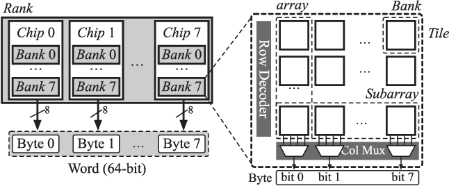
DDR4 SDRAM DIMM Organization

A channel is the physical connection between the memory controller and the DIMM, consisting of data and control/address buses. DDR4 DIMMs have a single channel, while DDR5 has two independent sub-channels per DIMM
A rank is a set of DRAM chips that share the same control/address and data buses and work together to service a command. Each chip supplies 8 bits, so to fill a 64-bit data bus, a single memory command results in responses from all eight chips in a rank
A DRAM chip consists of multiple bank groups. A prefetch is executed in one bank group, and another prefetch can be executed in another independent bank group, which reduces latencies compared to both commands executing in the same bank group
A bank within a bank group consist of a 2D memory array of cells, a row decoder and a column decoder. The array consists of rows, called word lines and columns, called bit lines. Each cell in the array stores 1 bit of data
A row decoder selects a row, called an opened row, to be latched into the sense amplifiers. A column decoder select a starting column for the burst transfer of the data to the bus
Accessing Memory
Read and write operations are a 2-step process. It begins with the ACTIVATE command, which is then followed by a READ or WRITE command
Activation
The ACTIVATE command is used to activate (or open) a row in a particular bank for a subsequent access. It reads cells charges from a selected row into the sense amplifiers
The address bits registered coincident with the ACTIVATE command are used to select the bank group, the bank and the row. This row remains active for accesses until a PRECHARGE command is issued to that bank or all the banks. This step is also called RAS - Row Address Strobe
A bank must be pre-charged before opening a different row in the same bank
Precharge
The PRECHARGE command is used to deactivate (precharge) the open row in a particular bank or the open row in all banks
Reading charge from the capacitors discharges them, destroying the information in each cell. The information must be put back into the DRAM array after an activation, otherwise the it is lost. Precharge is the process of deactivating the currently opened row and readying the DRAM to read data from a new row. It involves transferring the contents of the sense amplifiers back into the opened row’s capacitors and resetting the bit-lines
The bank(s) will be available for a subsequent row activation a specified time after the PRECHARGE command is issued, except in the case of concurrent AUTO PRECHARGE, where a READ or WRITE command to a different bank is allowed as long as it does not interrupt the data transfer in the current bank
Once a bank has been pre-charged, it must be activated prior to any READ or WRITE commands being issued to that bank
Read and Write
The READ command is used to read the data. The WRITE command is used to write the data
The address bits registered coincident with the READ or WRITE command are used to select the starting column location for the burst operation, determine if the AUTO PRECHARGE command is to be issued, and select the burst length. This step is also referred to as CAS - Column Address Strobe
Prefetching and Burst Transfer
Each DRAM chip transfers 8-bits of data in one-half clock cycle. Each DIMM consist of 8 chips operating in parallel to transfer 64-bits of data in one-half clock cycle
Read and write operations are burst oriented. They allow a burst of data to be transferred, starting from the specified column, while the row is still open. For a burst length of eight, a single read or write operation consists of eight corresponding 8-bit wide, one-half clock cycle data transfers per DRAM chip
Using this technique, called prefetching, a 64-bytes cache line is transferred in 4 clock cycles by issuing a single read or write operation, utilizing all 8 DRAM chips in parallel. Without prefetching, each operation to a DRAM chip would select a starting column, possibly pre-charging a new row, to transfer a 8-bits of data
A burst data transfer always accesses an 8-bytes aligned block of data. For example, a burst for any column address from 0 to 7 will return words from 0 to 7 in the specified burst order
Banks Interleaving
To allow multiple cache lines to be transferred in short succession, DDR4 uses bank interleaving
After a burst transfer is complete, a row in a bank has to be pre-charged (deactivated), and a new row activated. While one bank is busy handling pre-charge and activation, another bank can immediately start the burst transfer of the next cache line. This idea of interleaving allows for maintaining peak utilization of a shared data bus
References
- Computer Systems A Programmer’s Perspective, Global Edition (3rd ed). Randal E. Bryant, David R. O’Hallaron
- caching - Why isn’t there a data bus which is as wide as the cache line size? - Stack Overflow
- How does Computer Memory Work? 💻🛠 - YouTube
- Synchronous dynamic random-access memory - Wikipedia
- DDR5 SDRAM - Wikipedia
- Addressing the Memory Wall: 15-418/618 Spring 2015
- Lecture 24: Addressing the Memory Wall
- Computer Architecture A Quantitative Approach (6th ed). John L. Hennessy, David A. Patterson
- @depletionmode - Understanding DDR Memory Mapping
- Why is the burst order of DDR3 DRAM not sequential? - Electrical Engineering Stack Exchange
- DDR4 Tutorial - Understanding the Basics - systemverilog.io
- xdevs.com/doc/Standards/DDR4/JESD79-4 DDR4 SDRAM.pdf